Electrovibration is a haptic feedback effect that can make a smooth glass surface feel as though its texture is changing, without physically moving the surface. I wanted to understand whether that effect could be driven by a compact circuit with precise, programmable control over the waveform.
The idea started with my fourth-year undergraduate capstone project: a note-taking tablet that could reproduce some of the friction of writing on paper. My team’s first prototype was based on the TeslaTouch approach and used a transformer to generate the high-voltage signal applied to the indium tin oxide (ITO) layer of a surface capacitive touchscreen. It was a useful proof of concept, but the transformer was bulky, difficult to package inside a thin device, and best suited to a narrow range of waveforms.
A few years later, I returned to the problem with a different question: could I replace the transformer with a compact semiconductor circuit capable of generating arbitrary waveforms?
The resulting system starts with a 12 V supply and a waveform defined in software. An Arduino converts that waveform into a sequence of PWM duty cycles, while a custom two-layer PCB generates a 135 V rail, switches it according to the PWM signal, and filters the result back into a high-voltage analog waveform. I used a sine wave as the initial test case, but the same implementation can work for square, triangle, and custom periodic waveforms.
What is electrovibration?
Electrovibration changes the friction a person feels while moving a finger or conductive object across an insulated surface. A time-varying voltage is applied to a transparent conductive layer, such as indium tin oxide (ITO), beneath the surface. The resulting electric field creates a small attractive force between the surface and the user’s finger. The surface does not physically vibrate. Instead, the electrical force modulates the friction of a finger sliding across it, which can make the same piece of glass feel smoother, rougher, or textured.
The important part is that the sensation depends on the applied voltage waveform. Changing its amplitude or frequency changes the force at the surface. More complex waveforms create the possibility of more complex sensations. If that waveform can be updated in software, a touch interface could change its texture based on what is being displayed or where the user is interacting. A drawing application could make one region feel like paper and another feel smoother. Interface elements could have tactile boundaries even though the display itself remains flat.
For our capstone prototype, we based the high-voltage circuit on the approach described in TeslaTouch. A low-voltage (5V) sinusoidal signal was amplified and passed through a transformer to produce the 120V output required by the ITO surface. It was a practical way to demonstrate the principle, and a sine wave was enough for a proof of concept.
But the same circuit was a poor fit for the tablet we ultimately imagined.
The transformer added physical height and occupied valuable board area. Its behavior also depended on frequency, winding ratio, parasitic elements, and the capacitive load connected to its output. It worked well over the range it was designed for, but it did not provide a straightforward way to reproduce an arbitrary waveform. Signals containing fast edges or several frequency components would be shaped by the transformer rather than transferred perfectly to the surface.
I revisited the project a few years later with a different architecture in mind. Instead of asking one transformer to both increase the voltage and preserve the signal, I separated those jobs. A DC-DC converter would generate a high-voltage supply rail. A digitally controlled switching stage would define the waveform. A filter and output stage would then reconstruct and deliver that waveform to the surface capacitive touch surface.
This separation turns the high-voltage signal into something that can be programmed. The power stage determines the available voltage, while software determines how that voltage changes over time. A sine wave is still a useful first test, but it is no longer the only waveform the hardware is built to produce.
That became the goal of this project: build a compact, transformer-free electrovibration driver circuit whose output is defined in software, and determine whether a discrete implementation could eventually become part of a thin, programmable haptic display.
Design requirements
For the driver circuit to be acceptable, it needs to:
- Generate a high-voltage AC output of at least 110V peak-to-peak from a low-voltage DC supply without using a transformer. The supported frequency range of the output signal should be 60-600Hz.
- Reproduce a waveform defined in software as a sequence of PWM duty cycles.
- Control the output frequency and amplitude through the generated PWM signal.
- Produce an output that could be compared with the programmed waveform for amplitude, frequency, settling, ripple, and distortion.
- Fit on a compact, manufacturable two-layer PCB with accessible test points for bring-up and characterization.
System architecture
The system separates high-voltage generation from waveform generation. The power path produces a stable high-voltage supply, while the control path defines the desired waveform in software. The two paths meet at the high-voltage PWM stage before the signal is filtered and delivered to the touchscreen load.

Generating an arbitrary waveform
An arbitrary waveform is really just a sequence of voltage levels played back at a known rate. Rather than generate each level directly with a high-voltage digital-to-analog converter, I represented one period of the waveform as a lookup table and used pulse-width modulation (PWM) to encode each sample.
Representing the waveform as samples
A sine wave provides a useful example because its ideal shape and frequency are easy to calculate and compare with the measured output. I divided one period into 12 equally spaced samples. Each sample was shifted and scaled from the sine wave’s original range of -1 to +1 into a 7-bit PWM code between 0 and 127:
code[n] = round(127 × (sin(2πn / 12) + 1) / 2)
This produces the following lookup table:
{63, 95, 118, 127, 118, 95, 63, 31, 8, 0, 8, 31}
The same process is not limited to a sine wave. A triangle wave can be represented by values that rise and fall linearly, while a square wave alternates between the minimum and maximum codes. A custom texture waveform can be sampled in exactly the same way, provided its important features are within the bandwidth of the output stage.
Using PWM as a digital-to-analog converter
PWM represents a voltage level by rapidly switching between two states. The fraction of time spent in the high state is the duty cycle. After averaging, a 25% duty cycle represents approximately 25% of the available voltage range, 50% duty cycle represents half of the range, and 75% duty cycle represents three quarters of the range.
The intended Arduino timer configuration uses a PWM carrier of approximately 125 kHz. This is much faster than the desired 60-600 Hz output waveform. The firmware holds each lookup-table value for a fixed interval, then updates the PWM duty cycle to the next value. The high-voltage switching stage reproduces this pulse pattern at the 135 V rail, and the reconstruction filter removes the 125 kHz carrier while retaining the much slower change in average value.
The result is a high-voltage analog waveform whose shape follows the values stored in software.
Setting the output frequency
The output frequency depends on the number of samples in the table and the amount of time spent on each sample:
sample interval = 1 / (output frequency × samples per cycle)
For a 12-sample waveform, the timing across the target operating range is:
| Output frequency | Sample-update rate | Time per sample |
|---|---|---|
| 60 Hz | 720 samples/s | 1.389 ms |
| 100 Hz | 1,200 samples/s | 833 µs |
| 600 Hz | 7,200 samples/s | 139 µs |
At 100 Hz, for example, the firmware steps through all 12 entries every 10 ms. Each PWM code is held for approximately 833 µs before the next value is written.
The firmware implementation follows this basic loop:
for (int i = 0; i < num_samples; i++) {
    analogWrite(pwm_pin, waveform[i]);
    delayMicroseconds(sample_interval_us);
}
During bring-up, I could replace waveform[i] with a fixed PWM code to test the power, switching, and filtering stages independently. Once those stages were working, selecting a different lookup table changed the generated waveform without requiring any circuit changes.
There is still an important tradeoff. More samples produce a smoother representation of the desired waveform, but they also require more frequent duty-cycle updates. At the upper end of the 600 Hz target range, a 12-sample table must be updated every 139 µs. The PWM carrier must remain substantially faster than this update rate so that the filter has enough switching cycles to average each sample properly.
Circuit implementation
With the waveform represented as PWM, the circuit has three main jobs: generate a voltage level suitable to induce electrovibration, translate the 5V PWM signal into a high-voltage switching waveform, and deliver the reconstructed signal to the touchscreen through a protected output stage.
Input power and protection
The board is powered from a 12V barrel-jack input. A series fuse provides basic protection at the board boundary, while a 10 µF ceramic capacitor supplies local input decoupling for the switching converter.
The LT8331 enable pin is controlled by a 1 MΩ/287kΩ divider from the 12 V input. This keeps the converter disabled until the input is high enough to operate predictably and prevents it from continuing to switch as the supply collapses. I also brought the 12V rail out to a two-pin test header so it could be monitored during bring-up.
Generating the 135 V rail
I used an LT8331 boost converter to generate the high-voltage rail. The part integrates a high-voltage switching transistor, which allowed the converter to step 12V up to approximately 135V without an external transformer.
The power path consists of a 100 µH inductor, the LT8331 switching node, a Schottky rectifier, and a 1 µF output capacitor. A 1 MΩ/12.1kΩ feedback divider sets the output voltage near 135V. The circuit also includes a 100 nF soft-start capacitor to control how quickly the rail rises, a 154 kΩ timing resistor to program the converter’s switching behavior, and local decoupling for the LT8331’s internal supply.
The 135V target provides enough headroom to meet the requirement for an output of at least 110V peak-to-peak after losses in the switching, filtering, and output stages. The raw high-voltage rail is available at a test header so that startup, regulation, and ripple can be evaluated independently of the waveform path.
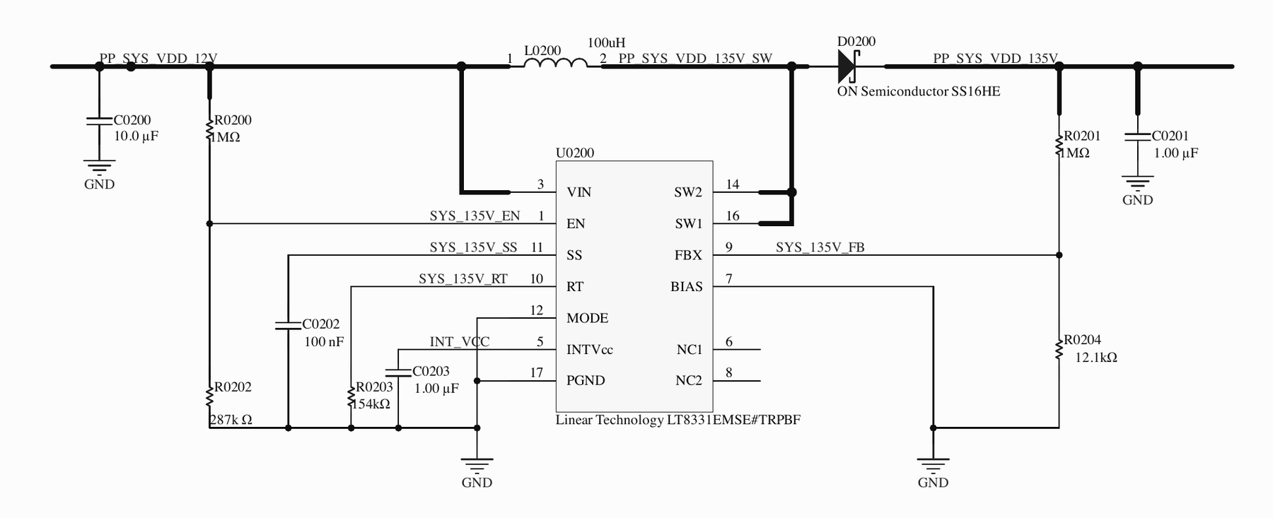
Figure 1. The LT8331 boost stage raises the 12 V input to a regulated 135 V rail. The feedback divider, soft-start capacitor, and switching components are shown here.
Translating PWM to the high-voltage rail
The Arduino cannot drive the 135V node directly, so its PWM output controls a discrete N-channel MOSFET. A 604kΩ resistor pulls the switching node toward the 135V rail, while the MOSFET pulls it to ground when turned on.
This makes the stage electrically inverting. A logic-high PWM state turns on the MOSFET and pulls the high-voltage node low. A logic-low state turns the MOSFET off and allows the pull-up resistor to raise the node toward 135V. The lookup table can account for this inversion by reversing the duty-cycle mapping in software.
The large pull-up resistance also limits the current drawn when the MOSFET is on. At 135V, the ideal current through 604 kΩ is approximately 223 µA. This is useful for a low-current electrovibration load, but it also means that the node’s rising edge depends strongly on the total capacitance connected to it.
Reconstructing the waveform
The PWM node includes five 10pF capacitors connected in parallel, giving a nominal capacitance of 50pF. Together with the 604 kΩ pull-up resistor, this forms a first-order low-pass response with a nominal corner frequency of approximately 5.3kHz.
That corner sits above the desired 60-600Hz waveform range and well below the intended 125kHz PWM carrier. The goal is to preserve the programmed waveform while averaging out the individual switching pulses.
The nominal resistor and capacitor values do not tell the whole story. The output-interface capacitance, MOSFET capacitances, PCB parasitics, and touchscreen load all appear at or beyond this node. The driver section also includes four high-voltage 1 µF capacitors connected to the filtered rail, so the installed component values and the way the stage is populated have a large effect on its dynamic response. This is why the final waveform has to be characterized with the real circuit and load rather than inferred from the 50 pF filter bank alone.
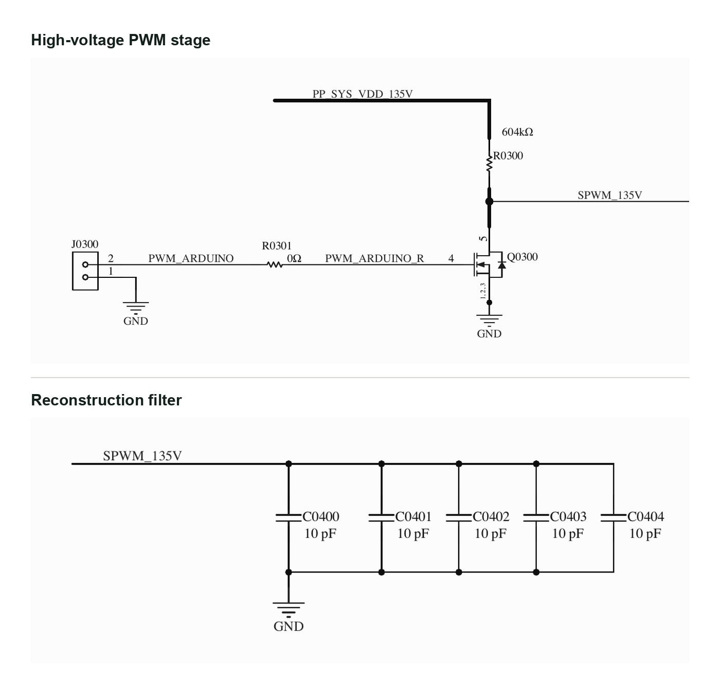
Figure 2. The Arduino PWM controls a low-side MOSFET connected to the 135 V rail. Five parallel 10 pF capacitors provide the nominal reconstruction capacitance at the resulting high-voltage PWM node.
Output driver and current sensing
The reconstructed signal feeds an LTC7000 high-side N-channel MOSFET driver. The LTC7000 is powered from the 12V rail and controls a separate high-voltage MOSFET between the filtered node and the output. In this prototype, the input command is held active so the device behaves as a protected high-side output interface rather than another waveform-modulation stage.
A 50mΩ shunt resistor allows the LTC7000 to sense output current. The sense lines are routed separately to the driver’s SNS+ and SNS- inputs, with a 100Ω resistor in the sensing path. The driver can report a fault when the sensed current exceeds its configured threshold. A bootstrap capacitor supplies the gate voltage needed to keep the high-side N-channel MOSFET on, while the timer and pull-up components define the fault response.
At the output, a 100kΩ resistor provides a path to ground so the node does not remain charged indefinitely after the driver turns off. The buffered waveform is also available at its own test header before it is connected to the ITO touchscreen.
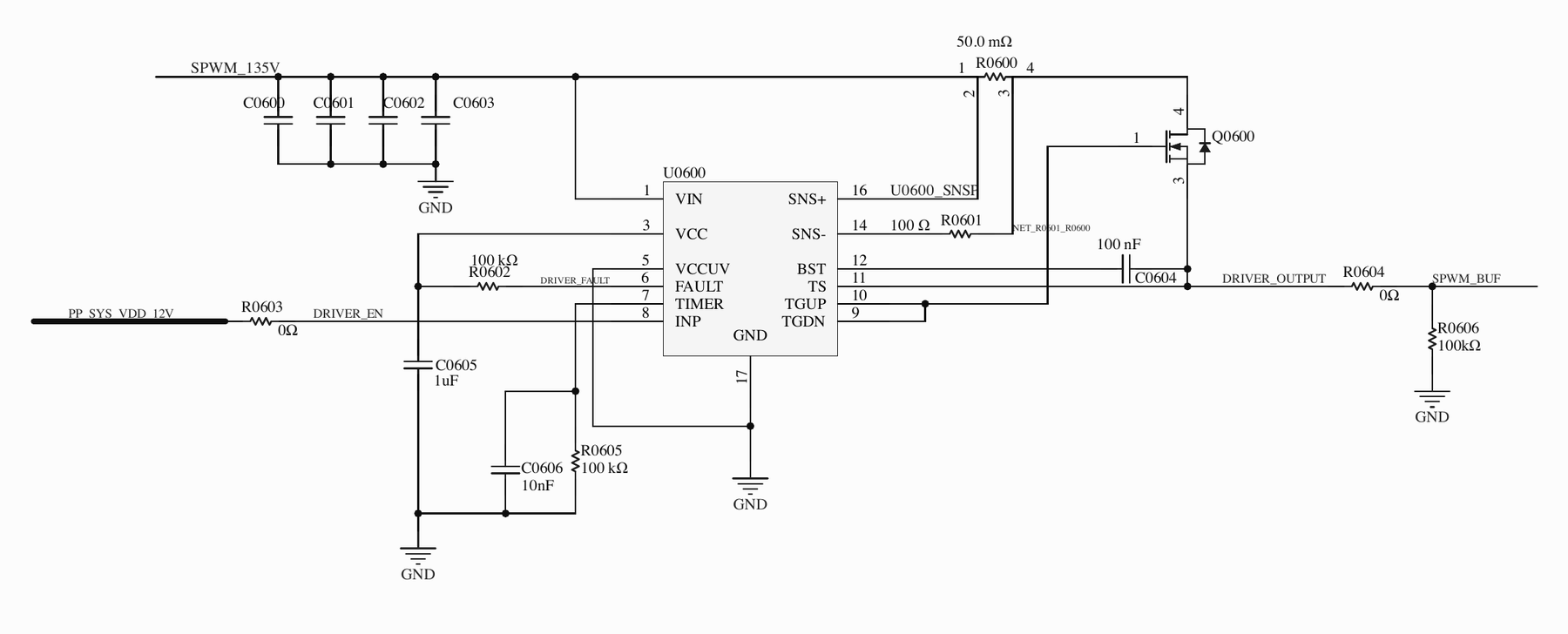
Figure 3. The LTC7000 controls the high-side output MOSFET, monitors current through the 50 mΩ shunt, and drives the final buffered waveform toward the touchscreen connection.
Designing for bring-up
I added five two-pin monitor connectors across the board: the Arduino PWM input, 12V input rail, 135V boost output, filtered high-voltage PWM node, and final buffered output. Each signal is paired with ground.
These connections make it possible to test the circuit one block at a time. I could first confirm the low-voltage PWM, then bring up the 135 V converter without the waveform stage, observe the high-voltage switching node, and finally compare the filtered and buffered outputs. That separation was especially useful in a circuit where a firmware error, converter problem, switching transient, or unexpected capacitive load could otherwise produce a similar-looking failure at the final output.
PCB implementation
I implemented the prototype as a two-layer PCB. The design did not contain dense digital routing, high-speed serial buses, or controlled-impedance signals, so additional signal layers would not have provided much value. Two layers reduced fabrication cost and kept the layout easy to inspect during bring-up.
All components are mounted on the top side. This simplified assembly and left the second layer available for a mostly continuous ground reference. I organized the board by function: the input connector and boost converter sit together near the top of the board, the PWM and reconstruction network occupy the center, and the output driver and current-sensing components form a separate group near the output connector. The monitor headers are placed around the outside so they remain accessible when the board is powered on the bench.
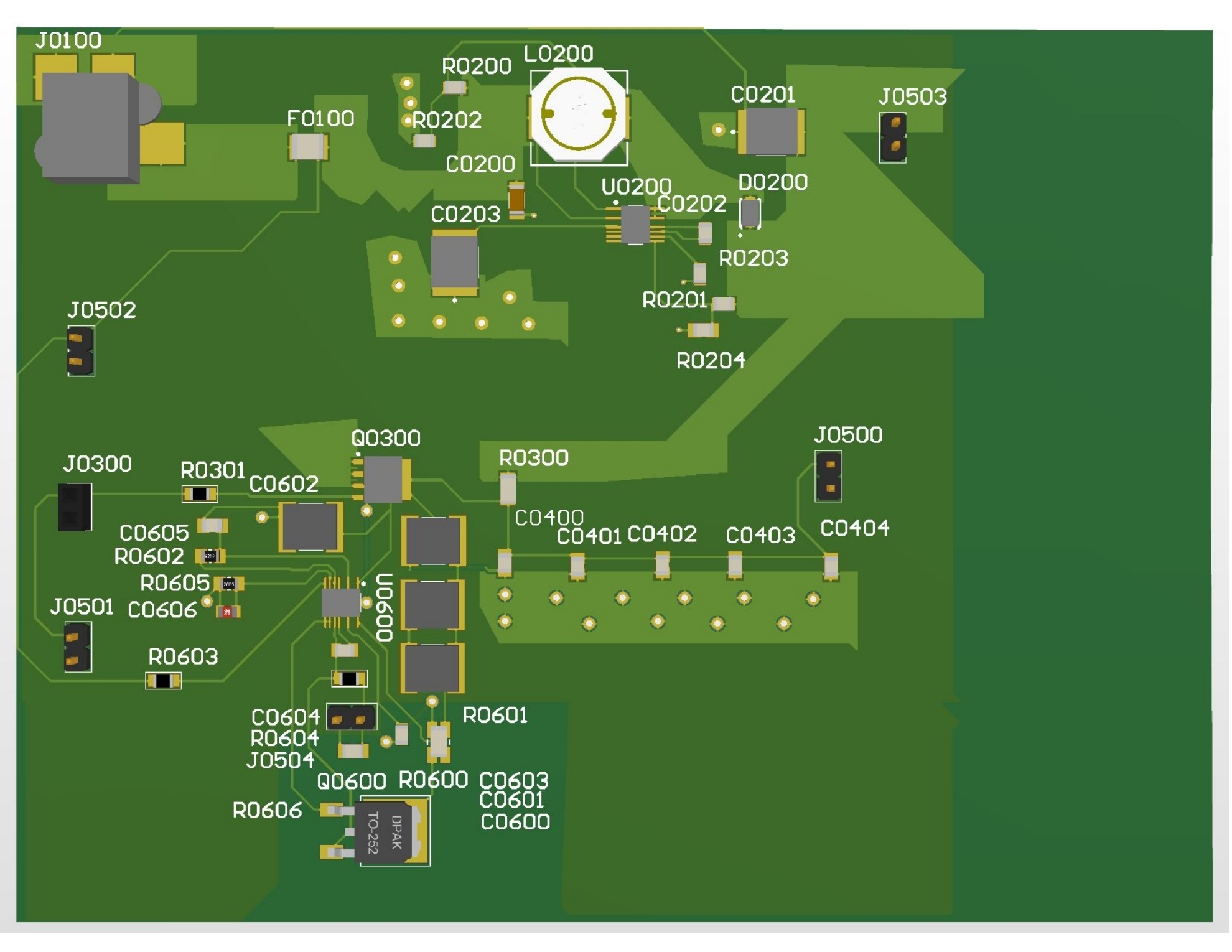
Figure 4. The populated top-side model shows the physical separation between the boost converter, PWM and filter network, and output-driver circuitry.
Power shapes and switching nodes
I used broad copper shapes for the 12 V input and the relatively static power rails. These connections carry converter current and benefit from lower resistance and inductance. The shapes also provide a direct path between the input capacitor, converter, output capacitor, and the circuits they supply.
Large copper areas are less helpful on nodes with fast voltage transitions. They increase parasitic capacitance and can couple switching noise into the rest of the board. I therefore kept the LT8331 switching loop—the inductor, converter switch pins, diode, and output capacitor—physically compact. The gate-driver loop around the LTC7000, bootstrap capacitor, and output MOSFET was treated similarly. Although the synthesized output is only 60-600 Hz, the board still has to handle the much faster edges produced by the boost converter and the 125 kHz PWM carrier.
Ground and return paths
The ground layer provides a short return path beneath most of the circuit. The important goal was not simply to cover the board with copper, but to keep switching currents local. The input capacitor returns close to the converter ground, while the gate-driver decoupling and timing components return near the LTC7000. This prevents large pulsed currents from sharing long sections of ground with the Arduino input or current-sense signals.
The current-shunt connections were routed as a dedicated sensing path rather than relying on the surrounding power copper. This reduces the error caused by voltage drop in the load-current path. I also kept the low-voltage PWM trace away from the 135 V switching region where practical.
Measurement and validation
The board is still in bring-up, so the results below are preliminary. Testing has verified the low-voltage waveform-generation path, but the 135 V supply must be corrected before the complete system can be characterized across the 60-600 Hz operating range.
Low-voltage waveform reconstruction
The 12 V input rail and the Arduino PWM signal were both verified at the board with an oscilloscope. The first capture shows the programmed 12-sample sinusoidal PWM sequence running at approximately 100 Hz. Each sample changes the PWM duty cycle so that its average value follows the sine-wave lookup table.

Figure 5. The 12-sample sinusoidal PWM pattern measured during the 12 V bench test. The repeating duty-cycle sequence corresponds to an approximately 100 Hz waveform.
After reconstruction, the duty-cycle sequence produces a stepped, sine-like voltage envelope. This demonstrates that the firmware, PWM timing, and basic reconstruction method work at low voltage.

Figure 6. The reconstructed response measured during the 12 V bench test. The stepped waveform follows the programmed sine-wave sequence at approximately 100 Hz.
These results validate the waveform-generation concept at 12 V. They do not yet characterize the final output amplitude, ripple, settling time, distortion, output current, or behavior with the ITO load.
High-voltage bring-up results
The PP_SYS_VDD_135V rail measured approximately 12 V rather than its 135 V target. The measurements collected during troubleshooting are summarized below.
| Test point or component | Measured result |
|---|---|
| 12 V input rail | 12 V; verified on the oscilloscope |
| Arduino PWM input | Present at the board; verified on the oscilloscope |
PP_SYS_VDD_135V | Approximately 12 V |
| L0200 | Approximately 12 V on both terminals while powered; continuity across the winding while unpowered |
| D0200 | Approximately 0.244 V in the forward direction and open-loop in reverse during diode-mode testing |
U0200 pin 1, EN | 2.7 V |
U0200 pin 3, VIN | 12 V |
U0200 pin 5, INTVCC | 3.4 V |
U0200 pin 9, FBX | 145 mV |
U0200 pin 11, SS | 647 mV |
U0200 pin 12, SYNC/MODE | Connected to ground |
| Q0300 drain | 0 V while its gate received the PWM signal and the pull-up rail was 12 V |
| 135 V rail to ground | No short detected while unpowered |
The boost stage has therefore not yet been validated. Ripple and load characterization will be performed only after the 135 V rail operates correctly and the incorrectly rated components have been replaced.
Part-selection errors
| Reference | Populated part | Selection error |
|---|---|---|
| D0200 | SS16HE Schottky diode, rated for 60 V reverse voltage | The diode must block approximately the full 135 V boost output. Its rating is below the intended operating voltage and leaves no margin for switching transients. |
| Q0300 | BUK9Y58-75B N-channel MOSFET, rated for 75 V drain-to-source voltage | Its drain can rise toward the 135 V rail while the MOSFET is off. Its rating is below the intended operating voltage and leaves no margin for switching transients. |
Both parts must be replaced with appropriately rated components before testing the circuit at its intended voltage. These are confirmed design errors, but the measurements collected so far do not establish that either component is the sole cause of the boost converter failing to start.